by Yee Wei Law - Wednesday, 29 March 2023, 10:18 AM
The increasing usage of cutting-edge technologies in safety-critical applications leads to strict requirements on the detection of defects both at the end of manufacturing and in the field [VDSDN+19].
Besides scan chains, test access ports (TAPs) and associated protocols constitute the fundamental test mechanism [VDSDN+19].
Among the earliest standards for test access ports is IEEE Std 1149.1a-1993, first drafted by the Joint Test Action Group (JTAG) in the late 1980s, and then standardised by the IEEE in the early 1990s [IEEE13].
The most recent edition of the standard is the 444 pages-long IEEE Std 1149.1-2013 [IEEE13].
This standard defines a test access port and boundary scan architecture for 1️⃣ digital integrated circuits and for 2️⃣ the digital portions of mixed analog/digital integrated circuits.
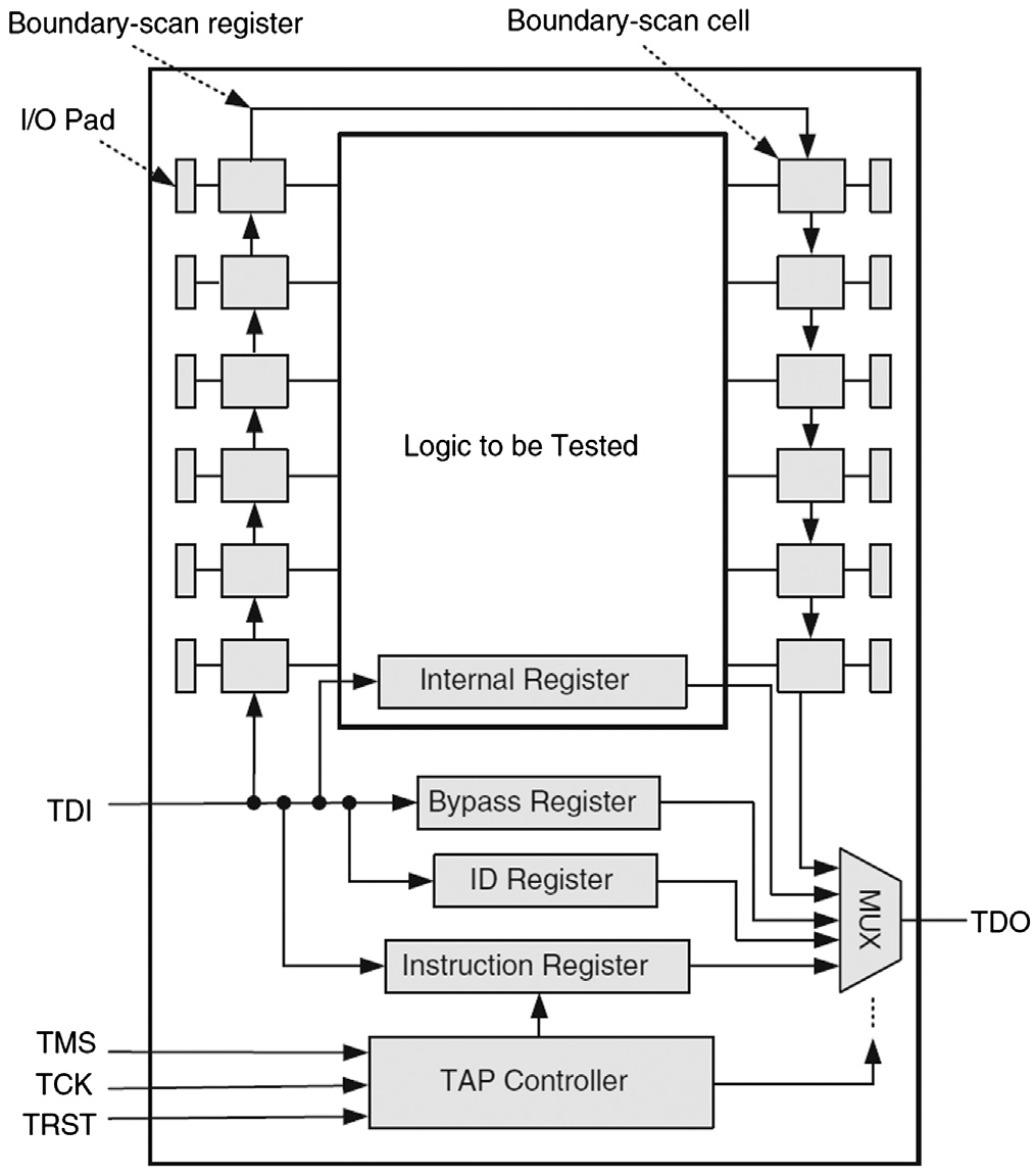
The architecture of boundary scan in Fig. 1 is responsible for controlling scan chains through a JTAG interface and an embedded hardware module [BT19, Sec. 3.6.3].
The technique of boundary scan involves the inclusion of a shift-register stage (contained in a boundary-scan register cell, see Fig. 2) adjacent to each component pin so that signals at component boundaries can be controlled and observed using scan testing principles [IEEE13, Sec. 1.2.3].
Instructions (not states) are loaded into the instruction register (IR), and depending on the instruction, a different data register (DR) is connected between the TDI and TDO terminals; for example, the BYPASS instruction connects a single flip-flop between the TDI and TDO ports [VDSDN+19, p. 96].
Fig. 1: The boundary scan architecture [BT19, FIGURE 3.19]. Note: TDI = test data input; TMS = test mode select; TCK = test clock input; TRST = test reset; TDO = test data output.
The boundary-scan register cells for the pins of a component are interconnected to form a shift-register chain around the border of the design, and this path is provided with serial input and output connections as well as appropriate clock and control signals [IEEE13, Sec. 1.2.3].
Fig. 2: A sample boundary-scan register cell [IEEE13, Figure 1-1].
If used for an input, data can either be loaded into the scan register from the input pin through the “Signal In” port, or be driven from the register through the “Signal Out” port of the cell into the core of the component design, depending on the control signals applied to the multiplexers (see Fig. 1).
If used for an an output, data can either be loaded into the scan register from the core of the component, or be driven from the register to an output pin.
The TAP controller in Fig. 1 implements the 16-state finite state machine in Fig. 3.
For example, Select-DR-Scan is a temporary controller state (i.e., the next rising edge of TCK makes the controller exit this state) in which all
test data registers (DRs) selected by the current instruction retain their previous state [IEEE13, p. 26].
If TMS is held low and a rising edge is applied to TCK, the controller enters the Capture-DR state and a scan sequence for the selected test data register is initiated.
If TMS is held high and a rising edge is applied to TCK, the controller enters the Select-IR-Scan state.
The instruction does not change while the TAP controller is in this state.
Fig. 3: The standard TAP controller state diagram [IEEE13, Figure 6-1].
Operationally speaking, the most important consideration for a security analyst, when assessing the security of a device, is finding a JTAG interface. Standard tools such as the Bus Pirate, JTAGulator and Open On-Chip Debugger (OpenOCD) can then be used to probe the device through this interface.
IEEE Computer Society, IEEE Standard for Test Access Port and Boundary-Scan Architecture: IEEE Std 1149.1-2013 (Revision of IEEE Std 1149.1-2001), 2013. https://doi.org/10.1109/IEEESTD.2013.6515989.
[RM19]
P. H. N. Rajput and M. Maniatakos, JTAG: A Multifaceted Tool for Cyber Security, in 2019 IEEE 25th International Symposium on On-Line Testing and Robust System Design (IOLTS), 2019, pp. 155–158. https://doi.org/10.1109/IOLTS.2019.8854430.
[RK10]
K. Rosenfeld and R. Karri, Attacks and Defenses for JTAG, IEEE Design & Test of Computers27 no. 1 (2010), 36–47. https://doi.org/10.1109/MDT.2010.9.
[VDSDN+19]
E. Valea, M. Da Silva, G. Di Natale, M.-L. Flottes, and B. Rouzeyre, A Survey on Security Threats and Countermeasures in IEEE Test Standards, IEEE Design & Test36 no. 3 (2019), 95–116. https://doi.org/10.1109/MDAT.2019.2899064.
[VL18]
G. Vishwakarma and W. Lee, Exploiting JTAG and Its Mitigation in IOT: A Survey, Future Internet10 no. 12 (2018). https://doi.org/10.3390/fi10120121.